The Amplifier Project
From March to June (of 2022) I designed and constructed a functional audio amplifier! I studied signal processing, acoustics, and electrical engineering to carefully draft three individual stages (filter, gain stage, output stage) and combine them to create a 5.5x gain amplifier!
Demonstrations
Amplifying "Weird Fishes/ Arpeggi" by Radiohead (one of my favorite songs of all time).
Amplifying raw voltage input from a signal generator (e.g. individual pitches).
Overview
This audio amplifier implements three stages: a band pass filter, a gain stage (amplifier), and an output stage.

The Filter Stage

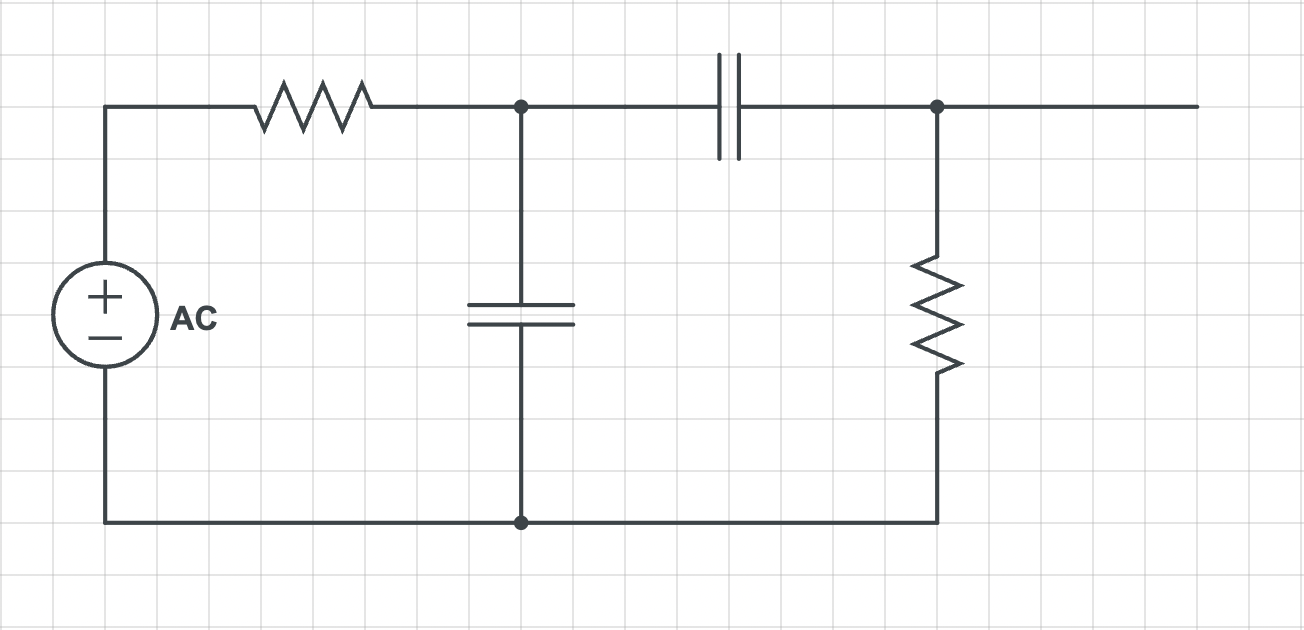
Circuit diagram illustrating the low-pass filter (left) and high-pass filter (right).
The band pass filter is comprised of two consecutive RC circuits. One acts as a low-pass filter and the other acts as a high-pass filter. Essentially, they only allow low/high frequencies (respectively) to pass through; the corner frequency values are determined by:
\[\large f_{c} = \frac{1}{2\pi(RC)}.\]The impedence of a capacitor in an AC circuit is as follows
\[\large Z = \frac{1}{i(2 \pi f) C}.\]With a given AC signal input at a given frequency we can determine the behavior of the output signal; furthermore, we can see how the arrangement of the two RC circuits differentiates the low-pass from the high-pass filter.
\[\large \lim_{f\to\infty} (Z)=0, \quad \lim_{f\to0} (Z)=V.\]Additionally, the presence of a capacitor in between the signal input and the gain stage adds another function: DC blocking. The capacitor allows AC signals (i.e. signals with non-zero frequencies) to pass through while blocking DC (signals with zero frequency) signals from interfering.
The Gain Stage

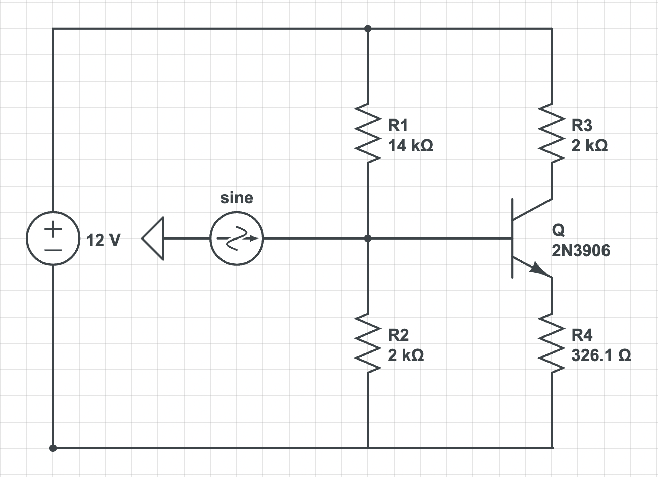
Circuit diagram illustrating the output stage.
The gain stage uses four resistors and an NPN transistor to produce a predicted 6x gain. I designed the circuit to implement voltage divider bias as it removes dependence on beta (highly variable due to a myriad of factors). Using resistors, we create bias voltages and generally fix the voltage difference across $\text{R}3$. The amp's gain is defined as the ratio between $\text{R}3$ and $\text{R}4$; we set the operating point to $3\text{mA}$ to achieve a $6\text{V}$ drop (the nominal point is $6\text{V}$).
With this design, the input signal (initially passed through the band-pass filter) is amplified to ~6x. The voltage swing is translate to be centered at $6\text{V}$ with a +/- $5\text{V}$ peak.
In characterizing the quality of this amplifier, I ran a fast-fourier transform and studied the harmonics to calculate the Total Harmonic Distortion (THD). Using the following equation, I found the THD which represents how much harmonic noise distorts the output signal; I aimed for a relatively low number.
\[\large \text{THD} = \frac{\sqrt{\sum_{n=2}^{\infty} V_{n(rms)}^2}}{V_{fund(rms)}}.\]The calculated THD for this amplifier is $2.359\%$.
The Output Stage

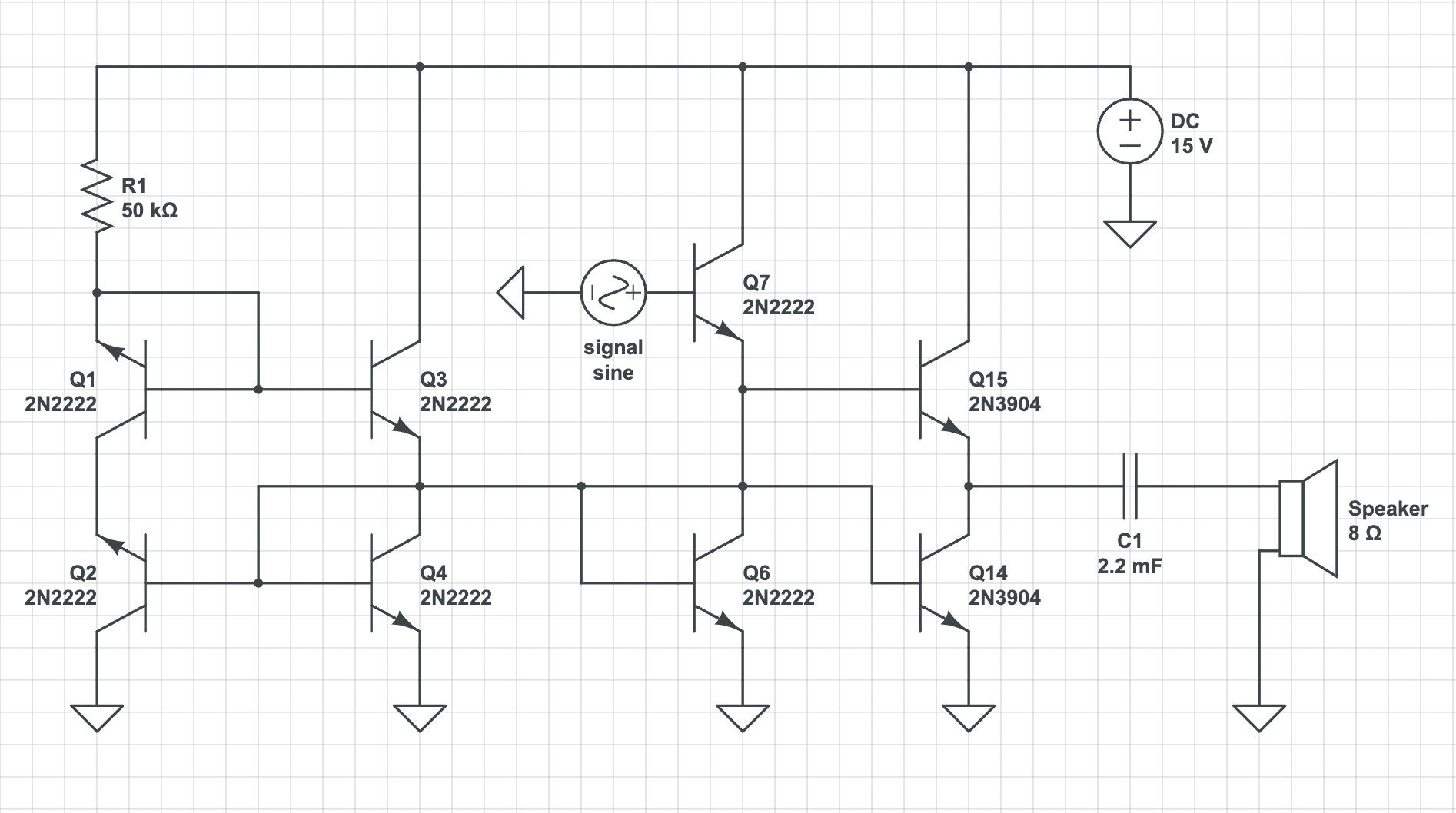
Circuit diagram illustrating the output stage.
The voltage gain stage properly amplifies the input signal; however, it lacks the current to drive the speaker. To solve this problem, I created an Emitter-Follower output stage (Q15), which maintains a ~1x gain while boosting the current into the speaker. However, when I connected this output stage to the voltage gain stage, I observed that the gain of the voltage stage itself dropped significantly.
The output stage maintains a high collector current ($~150\text{mA}$); this results in high base current ($I_c$ or $\beta$), where $I_c$ is the collector current and $\beta$ is the factor of proportionality between the base current and the collector current. From the datasheet, the minimum $\beta$ for a 2N3904 is $100$. Thus, the maximum base current we can apply is $\frac{150\text{mA}}{100} = 1.5\text{mA}$. The output stage (Q15) was loading the voltage gain stage collector terminal, thereby reducing the actual gain of the voltage gain stage.
To reduce the current load on the voltage gain stage, I added an additional gain stage (Q7). This stage was designed by using a 2N222 transistor with a minimum $\beta$ of $100$. Since it introduces another factor of $100$, it reduces the current load. This allowed the voltage gain stage to recover! Another design feature is the current mirror; this fixes the voltage drop across Q6 & Q14 Base - Emitter, which in turn fixes the current passing through the collector/output. Additionally, I needed to use heatsinks (both commercial and some DIY aluminum ones!) because the output stage transistors would heat up quickly. This caused thermal runaway which impacted the circuit--I countered this by monitoring the current from the DC power supply and using the heatsinks to keep temperatures relatively low.
The Final Circuit!
Showcasing the final circuit, including the filter, gain stage, and output stage.